LVDS-based IOs
Silicon Creations Bi-directional LVDS is in production from 90nm CMOS to 16/12nm FinFET and taped out in 7nm FinFET. This LVDS I/O is highly programmable and is an excellent IO for FPGA to ASIC conversions.
LVDS-based Interfaces
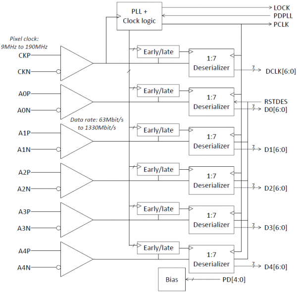
Based on this versatile LVDS circuit and our robust PLLs and CDR architecture we developed multiple uni-directional and bi-directional parallel source-synchronous interfaces for Chip-chip and Video data transmission. These interfaces can comply with custom chip-chip (or chip-FPGA) requirements or standards including FPDLink, FastLVDS, miniLVDS, FPD Link, Camera Link and OpenLDI. A dynamic phase alignment and robust word alignment architecture enables data rates exceeding 190Mpixels/s (1.34Gb/s in each lane) for FPD-link and up to 3.3Gbps/lane in some cases.
For more information on our LVDS Interfaces please download a product overview.
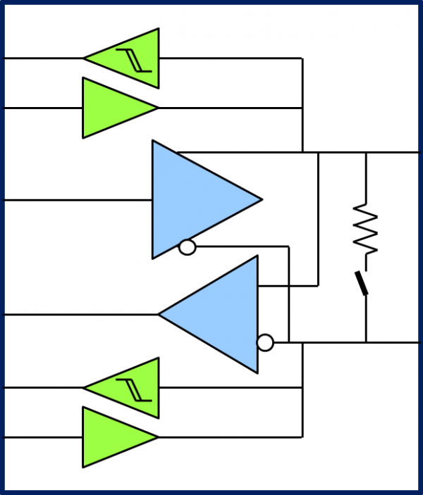
- TIA/EIA644A LVDS and sub-LVDS compatibility
- Receiver also compatible with LVPECL
- Operates over 2Gbps and up to 3Gb/s in some processes
- Trimmable on-die termination, can be enabled while Tx is operating for better signal integrity
- Independent LVCMOS input and output functions